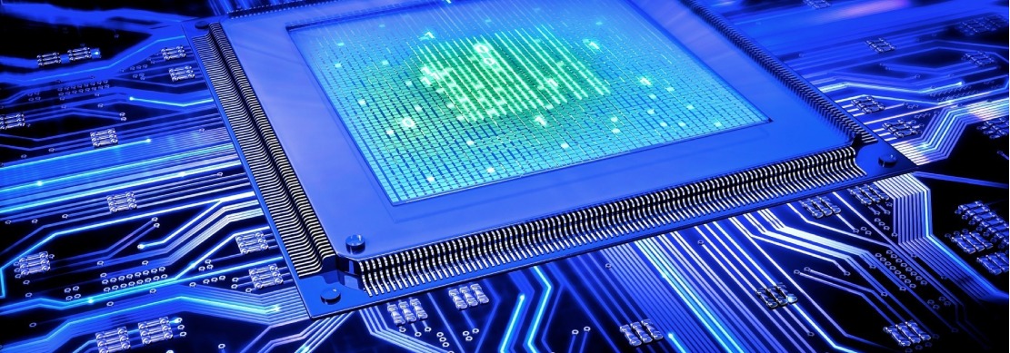
VLSI Layout & Backend
Focusing to provide best in class VLSI service form experience point of view, risk, schedule and price, KAL partnered with leading design houses to deliver complex, high performance & low-power RF/Analog Layout and Backend
Advanced Layout & Backend VLSI Services Driving Next‑Generation Silicon
As semiconductor designs push into sub‑5nm technologies and heterogeneous integration becomes the norm, backend VLSI engineering has evolved into a critical pillar of successful silicon realization. Modern SoCs demand aggressive PPA targets, multi‑domain power architectures, and signoff‑driven physical implementation flows that require deep backend expertise.
This edition highlights the technical advantages of leveraging specialized Layout and Backend VLSI services in advanced semiconductor programs.
Signoff‑Driven Physical Implementation for Advanced Nodes
Backend teams bring mastery of:
- Hierarchical and flat floorplanning
- Congestion‑aware placement
- Multi‑corner, multi‑mode (MCMM) optimization
- Advanced routing strategies for 5nm/3nm
- Clock tree synthesis with skew/power tradeoff tuning
These capabilities ensure that physical implementation aligns tightly with signoff requirements, reducing late‑stage ECO loops and improving schedule predictability.
Aggressive PPA Optimization Using Advanced Techniques
Modern backend flows rely on:
- IR‑aware placement and power grid synthesis
- EM‑driven routing and via optimization
- Leakage reduction through multi‑Vt cell selection
- Dynamic power reduction via clock gating and datapath restructuring
- Timing closure using path‑based analysis (PBA) and useful skew
These techniques enable backend teams to meet stringent PPA targets required by AI accelerators, high‑performance compute, and low‑power mobile SoCs.
Robust DRC/LVS/DFM Compliance for High‑Yield Silicon
Backend VLSI services ensure:
- Full compliance with foundry‑specific DRC decks
- LVS clean integration across hierarchical IPs
- DFM enhancements such as via redundancy, litho‑friendly routing, and density balancing
- Antenna rule mitigation and metal fill optimization
This reduces the risk of silicon failures, improves manufacturability, and enhances yield—especially critical at advanced nodes where margins are tight.
High‑Complexity IP Integration and Interface Closure
Modern SoCs integrate dozens of IPs with varying constraints. Backend teams handle:
- Multi‑voltage domain integration
- Level shifter and isolation cell insertion
- High‑speed PHY and SerDes placement optimization
- Memory compiler integration with custom routing constraints
- Power intent implementation using UPF/CPF
This ensures clean physical and logical integration across the entire chip, reducing late‑stage surprises.
Comprehensive Signoff Analysis and ECO Management
Backend specialists manage:
- STA across hundreds of MCMM scenarios
- IR/EM analysis using signoff tools
- Crosstalk‑aware timing closure
- ECO implementation with minimal perturbation
- Tape‑out preparation and GDSII validation
This end‑to‑end signoff ownership ensures that the design meets all electrical, physical, and reliability requirements before tape‑out.
Expertise in Advanced Packaging and 2.5D/3D Integration
As chiplets and heterogeneous integration grow, backend teams support:
- Floorplanning for interposer‑based designs
- TSV‑aware routing
- Thermal‑aware placement
- Power delivery optimization for multi‑die systems
This is essential for next‑generation HPC, networking, and AI architectures.
Scalable Engineering Resources for Complex Tape‑Outs
Backend VLSI service providers offer:
- Rapid scaling of physical design teams
- Access to engineers experienced with specific foundry nodes (TSMC, Samsung, Intel)
- Tool expertise across Synopsys, Cadence, and Siemens EDA flows
- 24/7 global execution models for schedule‑critical programs
This enables companies to handle peak workloads without long‑term staffing overhead.
Summary
Backend VLSI engineering is no longer a downstream task—it is a strategic enabler for achieving competitive PPA, ensuring manufacturability, and delivering reliable silicon at advanced nodes. With increasing design complexity and shrinking schedules, specialized layout and backend services provide the technical depth and execution efficiency required for successful tape‑outs.
Design Service:
- ASIC and FPGA design (Verilog/ VHDL)
- System-On-Chip (SOC) design
- IP Development
- Layout and backend design
- Transistor level design (PDK and IOs)
- ESD